Minimal Fab
Micro-fabrication and research-scale semiconductor lab solutions for advanced research and education.
Micro-fabrication and research-scale semiconductor lab solutions for advanced research and education.
Minimal fab is a unique Semiconductor Fabrication Solution developed in Japan by AIST (National Institute of Advanced Industrial Science & Technology), led by a consortium joined by a lot of semiconductor companies.
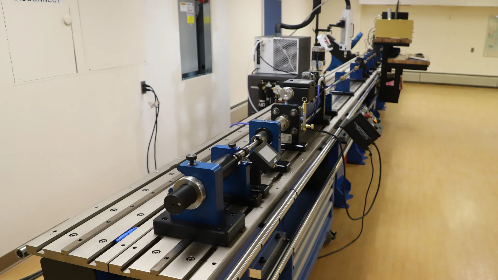
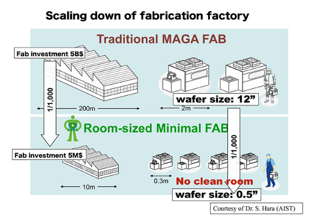
Minimal fab realizes high-variety and low-volume semiconductor fab consisting of ultra small tools by half inch size wafers, which has never been dreamed of on the conventional fab. While mega fab tools are built for production in high volumes with large number of chips from a single wafer, minimal fab is optimized for low-volume production.
Minimal fab meets the need for high-mix, low-volume production, making it ideal for research, prototyping, and specialized semiconductor applications.
Half inch size wafers for compact fabrication processes.
Optimized for specialized and research applications.
Minimal Fab offers significant advantages over traditional semiconductor fabrication facilities, making it ideal for research, prototyping, and specialized production needs.
Comfortably fits into the floor space of an ordinary office, no special facility requirements needed.
Operates without the need for expensive clean room facilities, reducing infrastructure costs.
Significantly reduces resource consumption compared to traditional semiconductor fabrication facilities.
Compact tools are ideally suited to low-volume semiconductor production and research applications.
Low investment as compared to Mega Fabs, making it accessible for research institutions and smaller operations.
Ideally suited to high-mix, low-volume production and multiproduct variable manufacturing.
Compare Traditional Mega Fab with Minimal Fab solutions
| Traditional Mega Fab | Minimal Fab | |
|---|---|---|
| Specifications | ||
| Wafer Size | 12" | 0.5" |
| Space Requirements | 200m² (Large facility) | Fits in ordinary office space |
| Clean Room Required | ||
| Investment | High (Mega Fab investment) | Low (Compared to Mega Fabs) |
| Production Volume | High-volume, mass production | Low-volume, high-mix production |
| Resource Consumption | High resource consumption | Minimizes resource consumption |
| Setup Time | Months to years | Weeks to months |
Timeline of Minimal Fab development from 2010 to 2019, showcasing key milestones in bringing this revolutionary technology to market.
The Fab lab research consortium was established in Japan to realize the Minimal Fab. The idea was to develop a facility for high mix low volume semiconductor devices in an ultra-short turnaround time (TAT).
Minimal fab development association was established as a national project by 22 core companies to accelerate the development and commercialization of Minimal Fab systems.
Yokogawa established the Minimal Fab Application Laboratory in April 2016 at Musashino-city, Tokyo to accelerate development and PR activities of Minimal Fab system.
In the year 2017, "Minimal Fab Promoting Organization" (MFPO) was established to accelerate commercialization of Minimal Fab technology.
AIST opened minimal fab in Tokyo Bay area for trial development by universities and companies in 2019, marking a significant milestone in making the technology accessible for research institutions.
Talk to our team about turnkey setups, instrumentation, training and AMC.